SHIMURA Takayoshi
SHIMURA Takayoshi
Dept. of Electronics and Physical Systems (interlocking prof.) Grad. School of Information, Production, and Systems
Specialization:Semiconductor materials and devices
Education
1987 B.Eng., Department of Applied Physics, School of Engineering, Nagoya University
1989 M.Eng., Department of Applied Physics, Graduate School of Engineering, Nagoya University
1992 Completed doctoral coursework without degree, Department of Applied Physics, Graduate School of Engineering, Nagoya University 1993, Ph.D. in Engineering, Graduate School of Engineering, Nagoya University
Career
1991–1992 JSPS Research Fellow (DC2), Japan Society for the Promotion of Science
1993–2007 Research Associate, School of Engineering, Osaka University
2007–2024 Associate Professor, Graduate School of Engineering, Osaka University
2024– Professor (fixed-term), Graduate School of Information, Production and Systems, Faculty of Science and Engineering, Waseda University
Research
Shimura Laboratory conducts research on advanced semiconductor materials and devices that support future information and communication technologies and efficient energy use. Building on semiconductor materials and device engineering, the laboratory takes an integrated approach ranging from fundamental studies of material growth and characterization to practical device applications with potential societal impact. This provides a broad learning environment both for students interested in the science of materials and for those who wish to contribute to future technologies and manufacturing.
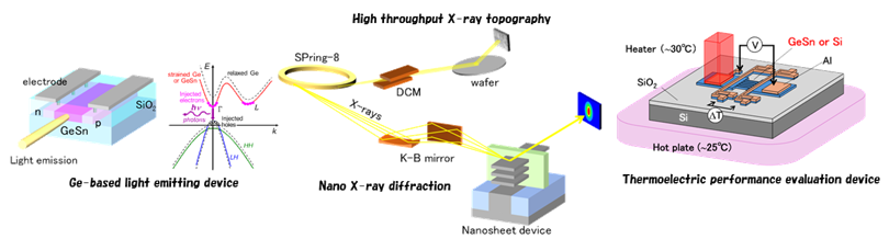
Our research focuses on three major areas. The first is the development of low-power optoelectronic integrated devices using group-IV semiconductors such as Ge and GeSn. By integrating electronic and photonic functionalities, we aim to enable next-generation technologies including high-speed communications, quantum information processing, biosensing, and high-speed image sensors. The second area is crystal characterization for wide-bandgap semiconductor power devices, particularly those based on SiC. Using advanced techniques such as X-ray topography, we analyze crystal defects in detail and contribute to the realization of high-performance, highly reliable power devices. The third area is the development of thermoelectric devices based on Ge-based materials. We focus on technologies that convert unused heat into electricity and pursue the creation of high-performance materials and innovative device structures for energy-harvesting applications.
Shimura Laboratory offers an intellectually stimulating environment for students who are interested in semiconductors and materials science, wish to learn across a broad spectrum from fundamentals to applications, and aspire to contribute to society through advanced technologies.
Research on semiconductor materials, crystal characterization, and device applications